Surface flatness measurements with optical flats
Flatness Measurements with Optical Flats
An optical flat is a glass, fused silica, Zerodur or sapphire disk polished to a high degree of flatness, typically within a few millionths of an inch, and is used as a reference to evaluate the accuracy of flat surfaces.
Measuring flatness using an optical flat entails direct contact between the specimen to be measured and the optical flat itself. Holding the surface of a high precision optical flat against the test specimen under monochromatic light creates visible light bands, which are formed by the air gaps where the two surfaces are not in perfect contact. These interference fringes show the contour of the surface under test. The light and dark patterns visually represent the flatness of the surface being tested, and it is the curve and spacing between these fringes which indicate the surface accuracy.
Disadvantages of Surface Flatness Measurements with Optical Flats:
- The optical flat is in intimate contact with the test sample, causing scratches in both.
- Test samples are placed on top of an optical flat for viewing with the help of a mirror. When placed horizontally, large diameter, thin parts can conform to the surface of the optical flat, causing an inaccurate reading.
- Classic Fizeau interferometers cannot measure flatness of thin, transparent glass 0.5mm (.020″) and thinner in a free-state, without applying an opaque coating to the opposite side of the thin part to be measured. This also distorts the specimen, and will cause an inaccurate reading.
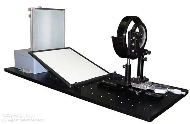
Introducing a New Flatness Measuring Instrument from Valley Design
Patented, our new non-contact interferometer, the Indars Interferometer, is designed to alleviate the problems inherent with using optical flats or Fizeau interferometers as discussed above. The Indars Interferometer has been specifically optimized for the flatness characterization of thin, transparent wafers, substrates and windows. Its unique design allows wafers to be positioned vertically, eliminating most bending forces applied by gravity and without necessitating the application of flatness distorting films.
For additional information on Optical flat interferometer see:
Optical Flat Interferometer
Please call or e-mail for further details.