The introduction of thin, transparent round and rectangular wafers and substrates for optoelectronic and semiconductor processing presents the problem of measuring their surface topography – flatness.
Since these wafers and substrates may be thin (typical thickness 0.5mm and thinner) and their diameter can be large (up to 300mm), the flatness measurement procedure can not be accomplished using traditional methods. Neither the Newton interferometer which requires horizontal contact with an optical flat possibly causing scratches in both, nor the classic Fizeau interferometer method which requires application of a coating on one side, can give a true flatness measurement.
Due to gravitational force, when positioned horizontally, thin wafers bend, causing considerable disturbance of the interferogram. The resulting fringe pattern, then, will not reveal a freeform profile of the wafer surface. To eliminate the influence of gravity on the surface profile, the wafer flatness should be measured when the wafer is in a vertical position in which most bending components of forces applied by gravity and supporting mechanisms of the instrument are eliminated.
When measurements for thin wafers and substrates are carried out on a classic Fizeau laser interferometer:
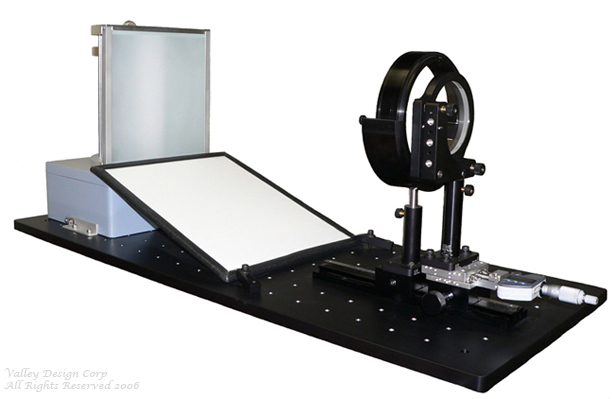
To address the issues inherent with these traditional methods, the new arrangement of the interferometer has been designed. The new Indars Interferometer scheme differs from others which are now in practice, by the vertical placement of the sample under test. Also, the need for application of distorting opaque film is eliminated.
The Indars Interferometer enables both elements, the part to be measured and the reference optical flat, to be kept parallel to each other at a distance on the order of coherence length of a light wave.
Please call or e-mail for further details.
Phoenix Park Business Center
2 Shaker Road, Bldg. E-001
Shirley, MA 01464
Email: info@valleydesign.com
Phone: 978.425.3030
Fax: 978.425.3031
Email: info@valleydesign.com
Phone: 831.420.0595
Fax: 831.420.0592


2025 Valley Design Corp. All Rights Reserved.
